Please note that this post is tagged as a rumor.
NVIDIA GH100 to be a big and power-hungry chip
NVIDIA Hopper shaping to be a monster of a GPU.
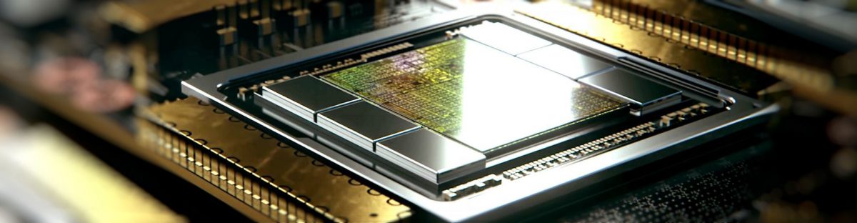
According to the latest report from @kopite7kimi, NVIDIA’s upcoming HPC accelerator called GH100 is to feature a massive die size of just slightly less than 1000mm² die. What this means is that the GPU might be up to 20% bigger than GA100 based on Ampere architecture.
Just yesterday we reported on a “Hopper” trademark dispute that NVIDIA is facing from a company using a similar name for its products. In case NVIDIA’s ongoing negotiations with the company called ‘Dish Network’ will not end in the next few weeks, NVIDIA might not be able to announce its new GH100 GPU at GTC 2022 in March.
DO NOT overreact. We know the actual die size will be significantly smaller than the package size.
But GH100>GA100 is confirmed. 😁— kopite7kimi (@kopite7kimi) January 29, 2022
Furthermore, it seems that the rumors about GH100’s Multi-Chip-Module design have been wrong. Now two leakers, including @kopite7kimi and @greymon55 both claim that GH100 is in fact a single-die design. However, it seems that is indeed a Hopper MCM design. This chip is supposedly called GH102 GPU.
https://twitter.com/greymon55/status/1487259506723594243
The GH100 is also expected to be a very power-hungry chip. Kopite earlier reported that the TDP might even reach 1000W which would require a very efficient cooling system. The company does, however, already offer a water-cooled data center GPU series called HGX, so that technically shouldn’t be a problem.
